A Gentle, Incrementally Comprehensive Introduction to GPUs: Curb your memory hierarchy!
New ASICs, TPUs, and fancier AI machinery is exciting. But to understand the excitement, let's go back to the basics and program a GPU.
In this post, we’ll take a shallow dive into NVIDIA’s CUDA programming model, with dedicated resources for those interested in going deeper. Using a software and hardware gaming PC setup you can purchase affordably (no fancy schmancy bank-breaking GPUs), we’ll write a kernel, which is a unit of software execution a programmer can run. We’ll go over what happens behind the scenes of a kernel at the compilation and execution stage, and gently expose you to the hardware processes like PCIE that the software rides on.
Finally, we’ll go under the hood of the kernel to witness an intricate interplay of software and hardware joining hands to deliver performance - doing things we’d normally do on a slower CPU, but faster. Buckle up, this will be a wild dash through a lot of really cool ideas.
Table of Contents:
Intro. Why we care about GPUs
A short, analogy filled story to understand the why behind GPU architecture
What happens when you compile on a GPU?
What happens when you run code on a GPU?
Understanding components of a GPU architecture that are often critical in pre-training
Applying that to understand typical hardware failure modes in AI
Writing a basic matrix multiplication kernel
Optimizing that basic matrix multiplication kernel
Appendix
Warps, and the silver lining
Do GPUs have a stack / heap / data layout like programs supporting virtual memory?
Why do you keep referring to “DMA”? Why do we care, as model architects, AI performance engineers, or computer architects?
An example of roofline analysis on GEMMs
What’s DDR? What’s GDDR? What’s HBM?
Introduction
There’s an emergence of a lot of different paradigms for designing hardware accelerators in the realm of ASICs. New opportunities like these open up systems questions, alongside hardware dilemmas related to programmability, i.e how to create a software interface that equips programmers with the tools to develop accelerated applications, and performance, the age-old question of how to make something run faster than before.
To think about those machines, we need to revisit the current state of the art that the systems community is well familiar with: graphics processing units (GPUs). Let’s talk today about, as of November 2025, the unquestionable king in the realm of GPU hardware.
The Story
For those who understand what CUDA is, feel free to jump on ahead. Stories are great, but I’m sure this isn’t the “technical meat” you’ve clicked onto this blog for. Warnings issued, let’s dive in. Let’s say you’re at the laundromat. But unlike the usual haul, you’ve got a truckload of dirty clothes of all sorts, and you want to finish this ASAP. What do you do?
A CPU can be thought of as a laundromat with 10 machines. They’re great for your normal haul … but take centuries on this newfound nightmare. If you’re anything like me, you’re probably looking for a bigger laundromat. Something a LOT bigger.
What about 100? That sounds a little better – we’re still slow, but we can do a lot more laundry than what we had a moment ago. We’ve got a lot of machines, though. And it would take a LOT of time to open the hatch for each one, dump a batch of laundry in, start the machine, and then repeat 100x.
Let’s do something crazy. Introducing the “Laundry-Dumpinator-9000”. Here’s how it would probably look.
And here’s what you can do with it.
Load 32 washers at once with your smelliest laundry. Yuck.
Retrieve all of your laundry at once.
Cool, but why not have the L.D. 9000 run on all 100 in one go? I’ll let you think about that while we move along. There’s a lot of great answers to this!
100 washers / 32 washers per L.D. 9000 gives us 3 L.D 9000 systems that we can feed our smelly socks into, with each “L.D. 9000 group” of at most 32 washers.
And that’s it! In our majestic quest to build the ultimate laundry time saver, we’ve come up with the blueprints for a GPU. A bird’s eye view, at least. Neat!
Let’s go back to GPUs. Instead of washing machines, we have CUDA cores. In computer design, our “laundry”, so to speak, is more along the lines of adding numbers, subtracting, and multiplying. Think of CUDA cores as doing just that. Just like we have 32 washers per “L.D. 9000 group”, we’ve got 128 CUDA cores per Streaming Multiprocessor in the RTX 4090 Laptop GPU, the one we’ll use in today’s experiments. That’s NVIDIA fancy for their group of processing entities. And like we have 3 L.D. 9000 groups, we have 24 SMs in our actual GPU. Like the L.D 9000, you can load data to all of these cores at once, and then get them to share their results at once, together through a synchronization step.
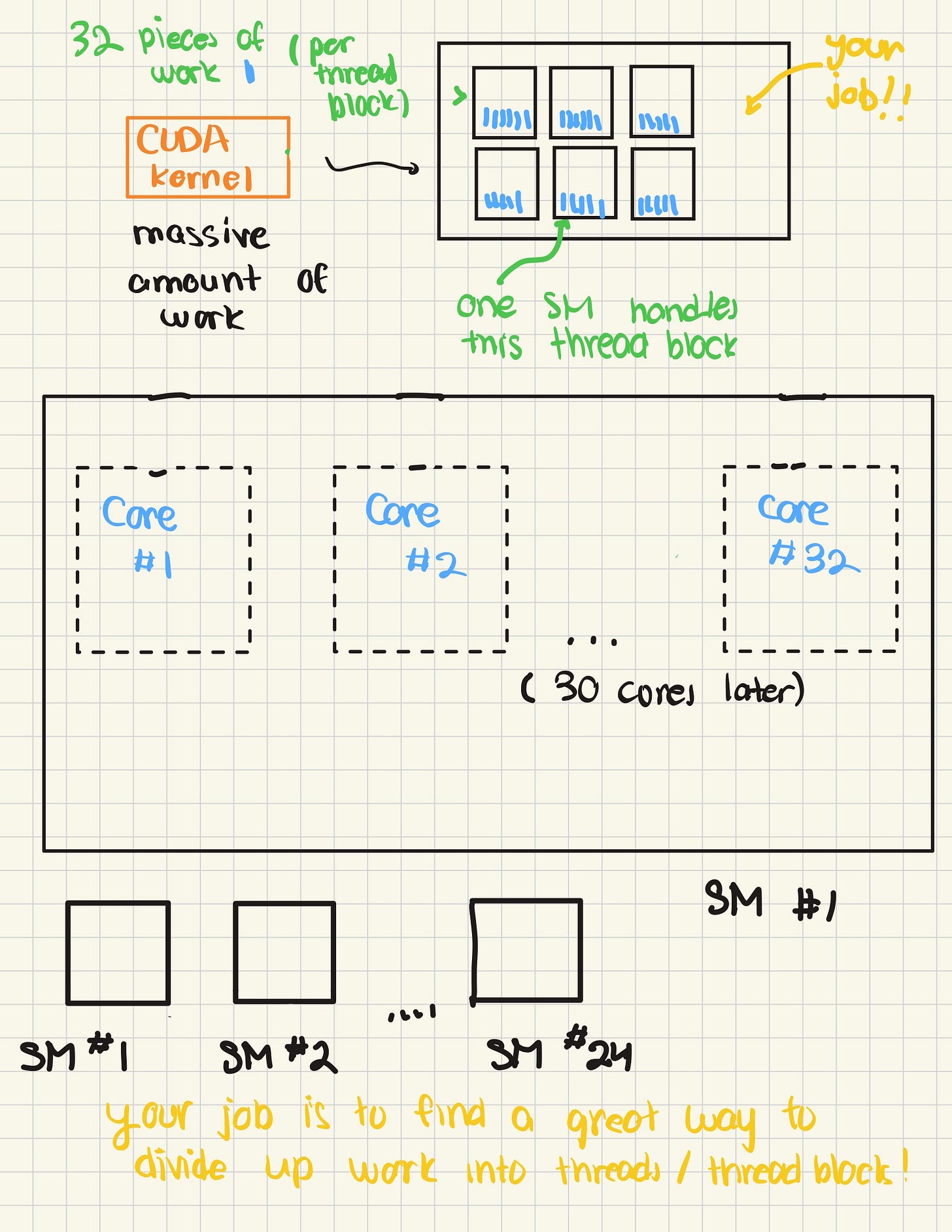
NVIDIA lets us tell what we want our processing units to do by writing a CUDA kernel. In the kernel, we have the freedom to choose how many workers per group, called threads, we need, alongside how many actual groups, called threadblocks, or blocks for short. Note that blocks aren’t the same thing as SMs! In terms of our analogy, think of blocks as a way of re-organizing the way you send laundry to the laundromat into groups.
You could be nice, and group your laundry into sets of 32, making it much easier for the L.D. 9000 when it has 32 washing machines, which may make it more efficient. Or some other way. The way you send work to the L.D. 9000 groups / set of SMs is completely up to you!
Morals of the story, in deeper detail:
We control our NVIDIA hardware using CUDA, which we can use to divide complex work into manageable blocks, and have threads within blocks run together at once to process work in a manner that’s highly parallel. We tell GPUs how to divide up their work into blocks they can process by writing out programs that we call CUDA kernels.
Each block that’s requested runs on a single streaming multiprocessor (SM). Once all the blocks have been processed, the GPU has “completed” its job.
Internal detail: Streaming multiprocessors usually like to process groups of threads in batches known as warps. The warp size, usually for NVIDIA GPUs, is 32.
Compilation: Creating a program that runs on the GPU
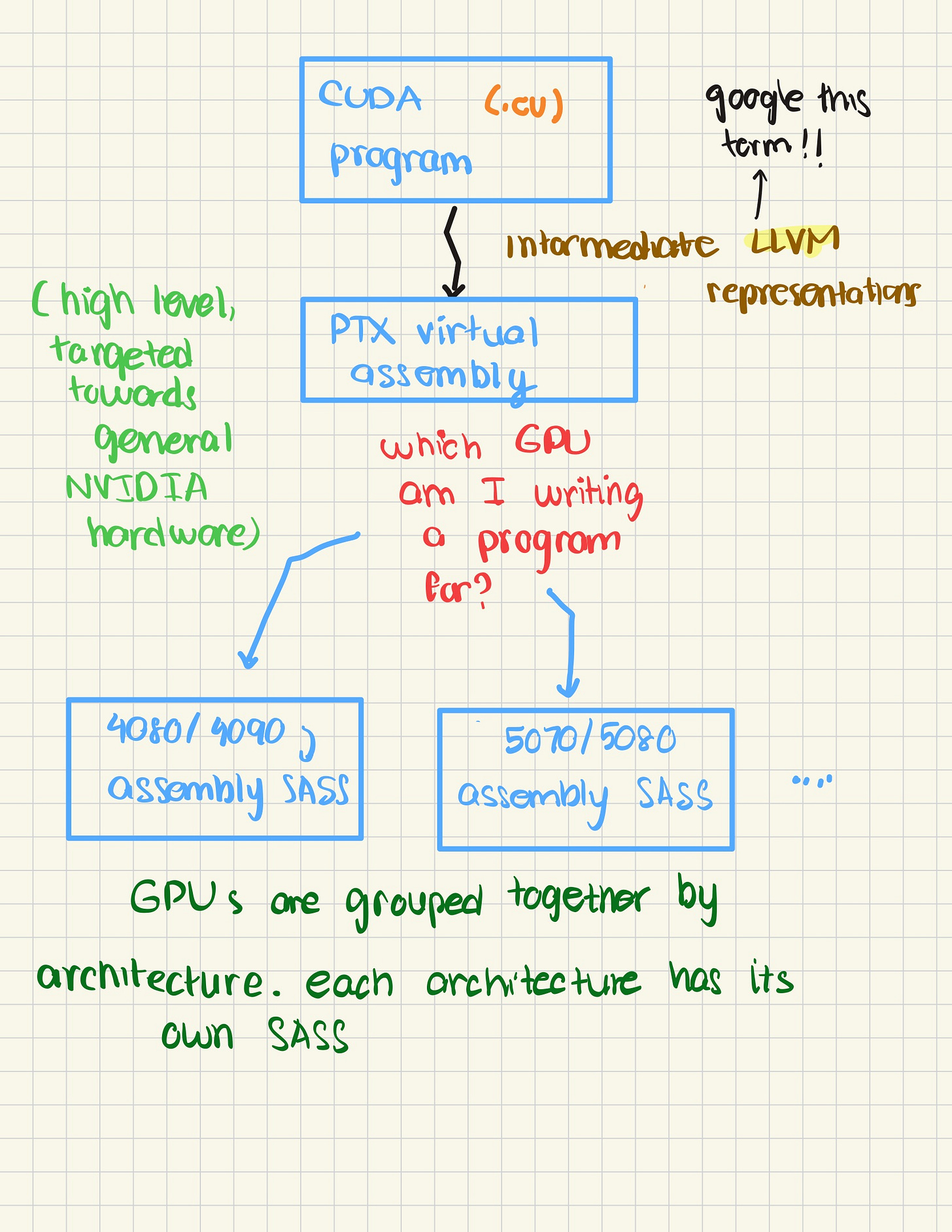
Like all code, we need to find a way to turn our human readable code into something that the GPU can understand? What does this call for? A compiler! NVIDIA’s CUDA software toolkit introduces nvcc, a compiler that takes programs written in CUDA, something that resembles C/C++ in syntax, and outputs assembly instructions that the GPU can run. But, nvcc is different from the compilers you might encounter. nvcc compiles CUDA files and transforms them into SASS.
But, what’s off? NVIDIA has a virtual assembly language, PTX. Why? That’s because NVIDIA doesn’t want to have to change instructions each and every time they create a new GPU. So, they have nvcc compile to PTX, and then ask the question – what instructions do I need to compile down to for this specific GPU?
Those GPU-specific instructions depend on the architecture family of the GPU. Each family has its own batch of architecture specific instructions that are incorporated into SASS. And based on the architecture, those specific instructions differ.
That’s why it’s important to share information on the software AND hardware. Each GPU has customized SASS instructions that enable it to do specific tasks really, really fast.
Execution: Ready, set, … PCIE?
Most software folks may stop and skip over this, and this often leads to more obscurity at scale, when you have processes powering clusters with hundreds of nodes, each containing a relatively constant number of GPUs, for AI. Let’s flesh out that hidden dirt.
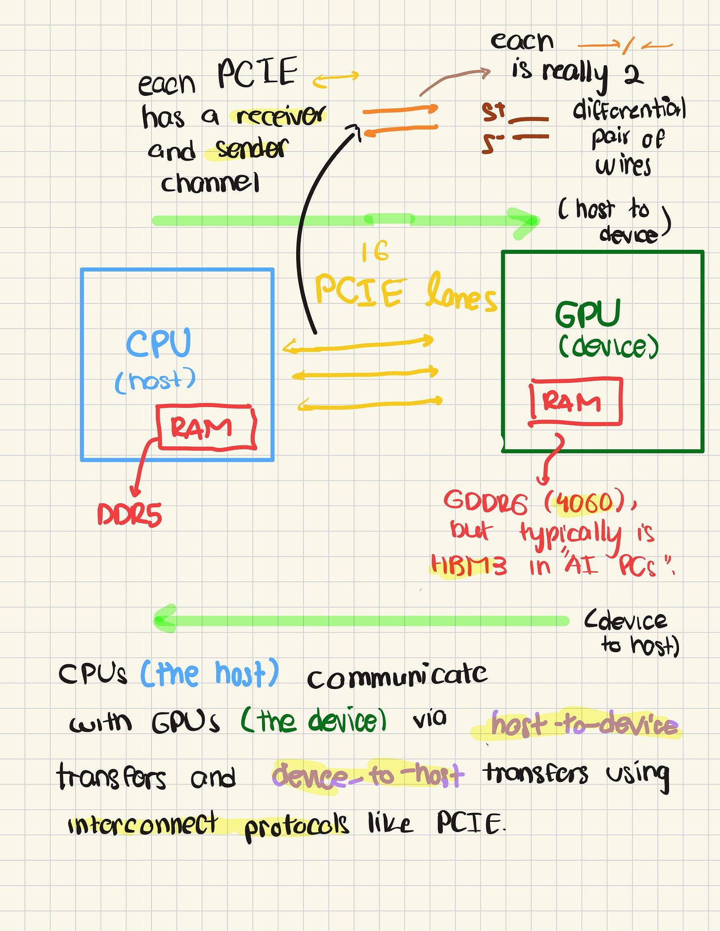
After the compilation step, you have a binary that strikingly resembles a binary that you’d typically run in C or C++. But, here’s the first challenge - you (i.e, your CPU), the host, need to run this binary on a completely different hardware (the GPU), termed the peripheral device in hardware lingo. How do we do this? To maximize data transfer speeds, we literally connect the GPU to the CPU, either through soldered lines, or wires with some hardware logic controlling this “bridge”, typically termed an interconnect. Enter Peripheral Component Interconnect Express (PCIE).
PCIE provides a standard for hardware connected to the CPU to effectively transmit and receive data. Typically, the PCIE is memory mapped – i.e, if the CPU issues “write” to the address, PCIE sends data to the peripheral, and a “read” to receive data.
Back to execution. Once you run the execution command, the CPU first processes the code as a normal program and loads it into RAM. But that’s where things become a bit different! At a high level, here’s what happens:
The CPU then checks the CUDA’s driver versions and hardware-side architectural information on CUDA. With this step, we’ve effectively initialized the CUDA driver and are ready to communicate with the GPU over our hardware PCIE interface.
A kernel launch is created, usually with fancy syntax that looks like `kernel<<<THREAD/BLOCK configuration>>>>`
Now, the CUDA driver sets the instruction cache for the GPU on the first call of the kernel. It literally ships binarized SASS to the GPU’s instruction cache (don’t worry if this term sounds scary, we’ll peek under the hood of a GPU as well).
Once the GPU has a place to find all the code to run, the CUDA driver sets up a packet to be shared through PCIE with data like:
Kernel function pointer – where in the instruction cache should we look for code to run
Thread / block / grid dimensions (think of grids as another way of grouping blocks)
How much shared memory each thread needs
Kernel arguments to expect
Stream / queue ID
The CPU sends data by telling the GPU where to look in the CPU’s own memory to retrieve the kernel pointer parameter data via DMA.
The GPU then uses its DMA engine to retrieve the contents of data arguments it seeks.
The CUDA driver sets a “valid” signal, letting the GPU know that legitimate work is pending
The GPU takes over and runs the kernel.
The CPU keeps running through the remainder of the instructions until a synchronize is requested, after which it polls GPU memory registers over PCIE and stalls until a completion flag is set.
The CPU retrieves data by telling the GPU to DMA the data back to a certain address in its own memory.
And … that’s it! A 50,000 foot view of what your CUDA program does in a nutshell. Each CUDA command is effectively bound by PCIE bandwidth when issuing commands, how long the GPU takes to process commands, and finally how blazingly fast your DMAs can ferry data to and from your CPU.
I’ve intentionally name dropped Direct Memory Access (DMA) engines across this to spark curiosity, but it’s not essential to understand if you seek to understand from a performance engineering (AI / software) side. If you’re hardware focused or marginally interested in how memory copies tick, check out the appendix!
Meet the beast: understanding GPU architectures at a high level
Let’s take a shallow dive into GPU architectures, looking at it from a minimalist view. We’ll try to delve into components that you only need to be aware of, or have an intuition for when debugging cluster hardware failures.
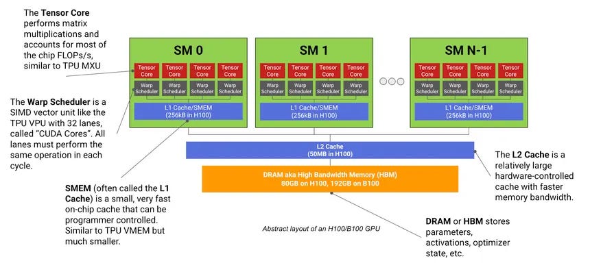
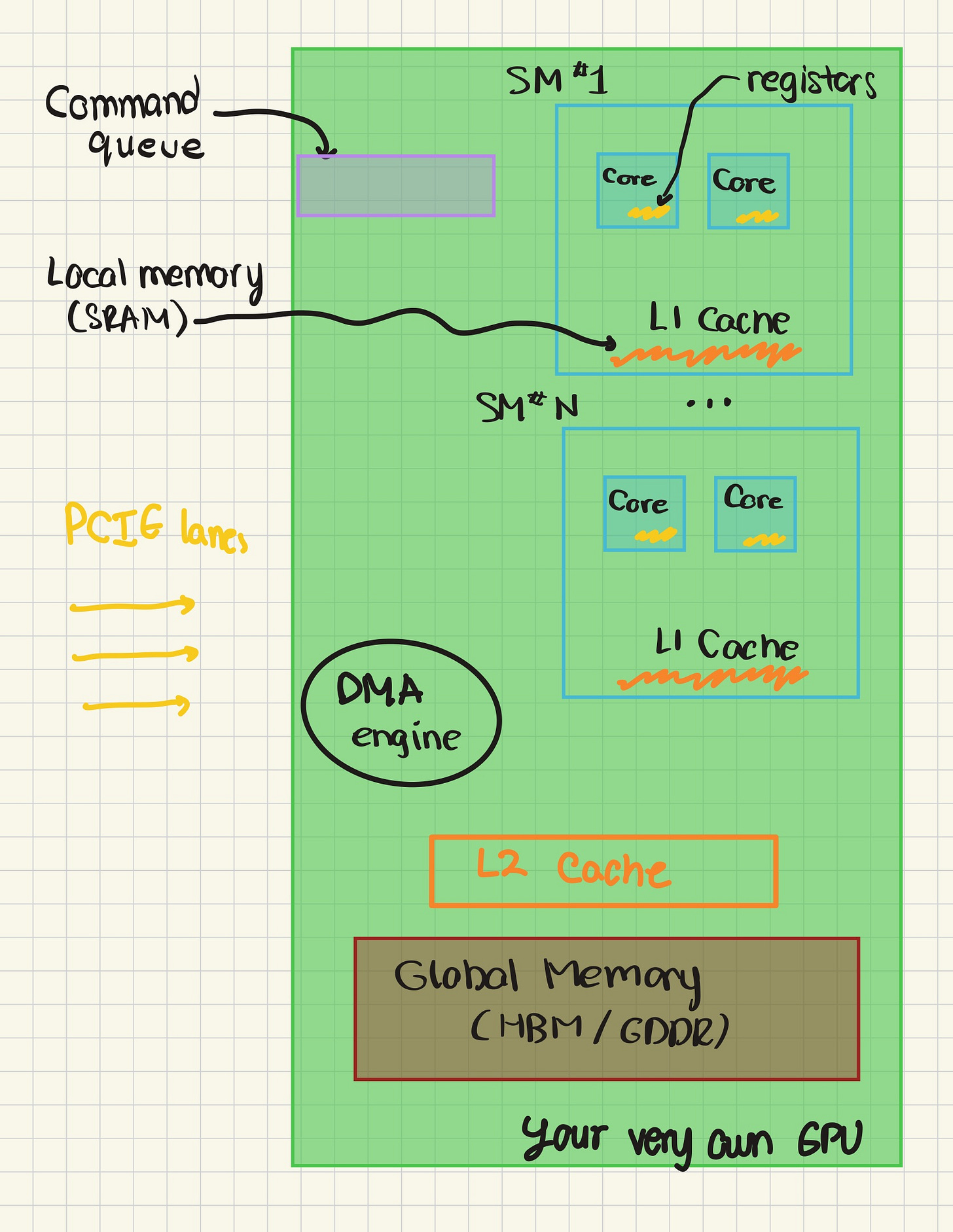
Let’s zoom out even further, to just the skeletal blueprints of a GPU.
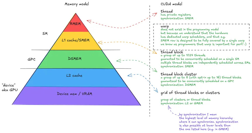
First, we need to understand a critical part of designing high performance kernels – the memory hierarchy of GPUs. The picture I’ve made above captures the absolutely necessary 60-70% of that, and for those interested in the full incarnation of memory, see this picture I sniped from Aleksa Gordic’s amazing blog on the same topic.
Generally speaking the memory hierarchy is defined by locality and access time. A single CUDA core is closest to registers, which, coupled with a static-logic based design for minimal access time, makes it the fastest to grab data from. Unfortunately, GPU designers need to be very judicious with the amount of registers they place on their GPU chips because of how expensive it is to fabric such logic. Going one level above, we find the L1 cache / shared memory layer. All CUDA and tensor cores within an SM can access the data stored just for the SM itself. Finally, we get to the global stage, which involves a system level L2 cache (aka the last level cache, LLC, L2C, or even L2$).
We add an L2 cache to speed up global memory accesses as the price to pay for accessing DRAM like HBM is just that significant. To recap, registers, L1, and L2 caches can be thought of as variants of static logic / SRAM, as they are based on storing data via logic based on cross coupled inverters. On the other hand, DRAM leverages dynamic logic, which makes it slower as its capacitor based. One must load the capacity with charge or perform a discharge to store a logical ‘0’ or ‘1’, making it orders of magnitude slower.
Practically applying what we’ve learned to understand GPU failure modes
For AI folks attempting to do large scale inference or pre-training, here’s where you get your ROI for reading all of this background setting. Typical hardware failures you should expect have to do with two parts of the GPU –
Command Queue Failures: Occasionally, non-determinism within GPU execution may lead to corrupting the commands sent over by the CPU.
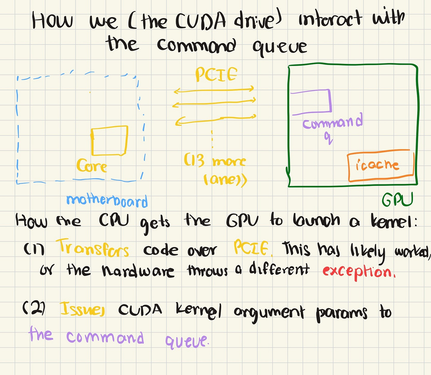
Here’s (in the image above) a brief recap. All of this parameter setting and GPU execution work is done by software called the CUDA drivers. Essentially, your software directs the CUDA driver to make some task on the GPU happen whenever it calls the CUDA API. I’m introducing this as it’s important to identify which piece of software to fault in case we know it’s a software issue.
This is pure speculation as CQE errors can depend in what caused them, but if the software is the issue, it’s generally because somewhere, the state of the CUDA driver was corrupted, or malformed as a result of receiving some challenging directives.
However, it’s equally possible that the hardware has been corrupted. This is significantly less likely — most hardware is designed with some level of redundancy, so definitely try to restart your CUDA drivers a couple times before asking for support on the notoriously slow NVIDIA forums.
TLDR: Cluster recommendations are to perform a point reboot. If the error persists, ask for help from the hardware vendor.
Memory - SRAM / DRAM - Error Correcting Code Failures: When a GPU is executing code, requests to memory will often contain parity bit checksums. If, at any point for data in memory, the parity bits don’t represent the data stored, data has generally been corrupted at the hardware level. If too many corruptions happen, the GPU may throw it’s hands up and bail on the computation entirely.
It’s hard to pinpoint a cause for these errors, as the problem can be with the stability of the data within the DRAM 1T-1C cell, or external datacenter factors that repeatedly cause corruption on the piece of hardware. Most hardware should have redundancy baked in, so expect this to be pretty rare.This happens very infrequently, and large, consecutive batches of these errors can indicate faulty hardware.
Now, we’ve honestly overkilled the amount of context we need to write a kernel. If you want more, feel free to dive deeper into HBM vs DDR / GDDR to go beyond the memory terminology. To make sure that this blog post doesn’t turn into a 300-page book, let’s try to understand a really simple example of a kernel, and how it may relate to the underlying GPU.
Let’s write a kernel!
The most fundamental computation in a GPU, depending on the person you ask, is generally either the vector dot product, or a matrix multiplication. Let’s try writing a matrix multiplication kernel. All code will be linked to my blog posts repository here.
I’m of the philosophy that the general approach to solving technical problems is to start with a really easy to understand approach that may be a tad bit inefficient, and then incrementally resolve inefficiencies through (1) deep and careful understanding of the problem, and (2) research on candidate solutions. For the sake of your time reading this, we’ll just make an easy solution and try to understand what it does deeply.
Let’s define our problem. Given a pointer to a 2D array A, and a similar pointer to 2D array B, compute C = A x B.
The problem can feel incredibly scary at first, but the secret is to lean in on nice abstractions that CUDA has provided you with when creating threads and blocks. Let’s build this step by step, and introduce thread and block concepts as they’re needed.
How do we humans do matrix multiplications? Let’s take a really simple example.
What do we do here? We compute a dot product. Well, a dot product doesn’t sound too bad to compute. We just loop over two arrays and multiply individual elements together. Something like this.
for(int i = 0; i < N; i++) {
    C[i] += A[i] * B[i];
}
Great! Now, let’s talk about how we can access kernel threads and blocks using CUDA’s API. The kernel code we write lets us control what the GPU does in each thread, with minimal support for letting threads within blocks communicate with each other. Thanks to the API, we can group threads and blocks into spatial dimensions. Instead of having a single thread index between 0-3, we can have thread indices in the x direction from 0-1 and y direction from 0-1. That makes it a lot easier to compute matrix multiplication entries. Now, we can have each thread (i, j) do the for loop we suggested above with the rows of A based on index i and columns of B based on index j.
That leads to something looking like this (full code here ) -
#include <cuda_runtime.h>
#include “stdio.h”

__global__ void matrix_multiplication_kernel(const float* A, const float* B, volatile float* C, int M, int N, int K) {
    int y = blockIdx.x * blockDim.x + threadIdx.x;
    int x = blockIdx.y * blockDim.y + threadIdx.y;


    if(x < M && y < K) {
        // printf(”Thread indices entering if - %d %d\n”, x, y);
        for(int i = 0; i < N; i++) {
            C[x * K + y] += A[x * N + i] * B[i * K + y];
        }
    }
}

// A, B, C are device pointers (i.e. pointers to memory on the GPU)
extern “C” void solve(const float* A, const float* B, float* C, int M, int N, int K) {
    dim3 threadsPerBlock(16, 16);
    dim3 blocksPerGrid((K + threadsPerBlock.x - 1) / threadsPerBlock.x,
                       (M + threadsPerBlock.y - 1) / threadsPerBlock.y);

    matrix_multiplication_kernel<<<blocksPerGrid, threadsPerBlock>>>(A, B, C, M, N, K);
    cudaDeviceSynchronize();
}
I’ve just dumped a bunch of code on you, let’s dissect. First, let’s talk about the solve function. Here, we define a thread grid of 16 x 16 threads within a block. Remember that our 4060 GPU has a max thread count of 1024, so this is legal. Notice how also have the option to arrange the blocks by x/y coordinates into a “grid”. What this code is effectively doing is tiling the matrix into smaller chunks of work that can be computed in a block.
We can run as many blocks as we like on the GPU, but we can only run a certain number of thread blocks at once in parallel. This is what we like to call the compute bound. In the case for our 4060, we can get a pretty rough upper bound for our program.
(24 SMs total / 1) * (1024 threads / SM) * (1/256 threads requested) = 96 blocks in parallel.
Fortunately, a 2x2 matrix multiplication, which I’ll abbreviate to matmul in the future, only has 4 entries. That means we only use one thread block, but we waste a lot of threads.
Out of the 256 blocks in our kernel, only four are in use. So, we’ve unnecessarily hogged = 256 - 4 = 252 threads. It’s important to note that with most matrix multiplication kernel thread/block configurations, you’ll still find some waste like this. We call this issue tiling inefficiency.
Cool, back to the code. The next couple lines are a lot of fancy syntax for launching a CUDA kernel with our threads and blocks. Feel free to use your friendly neighborhood LLM to dive deeper into syntax.
With that, we dive into the meat: the matrix_multiplication_kernel method, which is our CUDA kernel. At a high level, we define indices to obtain the row of A and column of B we wish to multiply. Then, we perform the actual dot product, after making sure that only the thread indices we want are doing the computation – sometimes we have more threads than we do matrix entries for the tile.
And that’s the entire kernel. Feel free to clone my git repository and run the kernel with the benchmarking script, provided you have an NVIDIA GPU, access to Google Colab, or one of many GPU cloud vendors out there.
But is this the best we can do? Let’s revisit the memory hierarchy. Each time we do an accumulate, we’re doing the following operations (assuming no cache):
Load an entry from the A vector from global memory
Load an entry from the B vector from global memory
Load an entry from the C vector from global memory
Multiply the entry from A * entry from B, and accumulate into C
Write back the value of C to global memory
Do we really need to write C back to global memory each and every time? No! Going to memory means you pay the largest price, and with this code, we’re paying it in the worst way possible. Let’s look at the actual SASS snippet code for this (with as many nvcc optimizations disabled as possible to get an idea of the raw logic) -
LD.E.CV R14, [R14], P0 ;           // Load C[x*K+y] (VOLATILE)

// Add to C

FADD R14, R14, R12 ;               // R14 = C + (A*B)

// Store back to C[x*K+y]

MOV R13, R16 ;

MOV R15, R17 ;

LEA R12.CC, R13, RZ ;

LEA.HI.X P0, R13, R13, RZ, R15 ;

MOV R12, R12 ;

MOV R13, R13 ;

ST.E.WT [R12], R14, P0 ;           // Store C[x*K+y] (VOLATILE)
See the LD.E and the additional ST.E? These are redundant, and don’t need to be done per iteration.
Making them go brrr…
Instead, let’s use registers to avoid writes. We’ll define a float register sum (defining variables in kernels generally allocates them to register memory), and then accumulate using that.
Something like this
#include <cuda_runtime.h>
#include “stdio.h”

__global__ void matrix_multiplication_kernel(const float* A, const float* B, float* C, int M, int N, int K) {
    int y = blockIdx.x * blockDim.x + threadIdx.x;
    int x = blockIdx.y * blockDim.y + threadIdx.y;

    float sum = 0.0f; // NEW!

    if(x < M && y < K) {
        for(int i = 0; i < N; i++) {
            sum += A[x * N + i] * B[i * K + y];
        }
        C[x * K + y] = sum;
    }
}

// A, B, C are device pointers (i.e. pointers to memory on the GPU)
extern “C” void solve(const float* A, const float* B, float* C, int M, int N, int K) {
    dim3 threadsPerBlock(16, 16);
    dim3 blocksPerGrid((K + threadsPerBlock.x - 1) / threadsPerBlock.x,
                       (M + threadsPerBlock.y - 1) / threadsPerBlock.y);

    matrix_multiplication_kernel<<<blocksPerGrid, threadsPerBlock>>>(A, B, C, M, N, K);
    cudaDeviceSynchronize();
}
Check out the difference! Ideally, it would be much faster. Ideally.
In reality, it’s hard to disable all of the caches, in particular the LLC. On the first request, from memory, the NVIDIA L2 cache stores a line in units of 32 bytes (B). Our matrices only have 4 elements, and we’re the float datatype, which is equivalent to fp32, which means 4 bytes per value. So loading A and B would require requesting 4 elements * 4 bytes / element * 2 matrices = 32 bytes. That’s one sector.
So, the cache can serve all of our read and write operations with one load from memory, which we anyways need to gather the data. NVIDIA’s cache has a write back policy, meaning it only writes data back when we absolutely need to. That generally only happens when the cache is storing too much information, and needs to evict data by writing the results it has saved to memory.
So all, in all, our optimizations ended up getting thwarted by well-placed caching. But it’s the learning that counts, amirite? Or the dirty laundry you likely put away after reading this. 😀
Appendix
Warps
In fact, we didn’t touch upon one critical area: how threadblocks are mapped onto warps. Below, I’ll provide a brief walkthrough of how the warps would end up executing 256 thread blocks
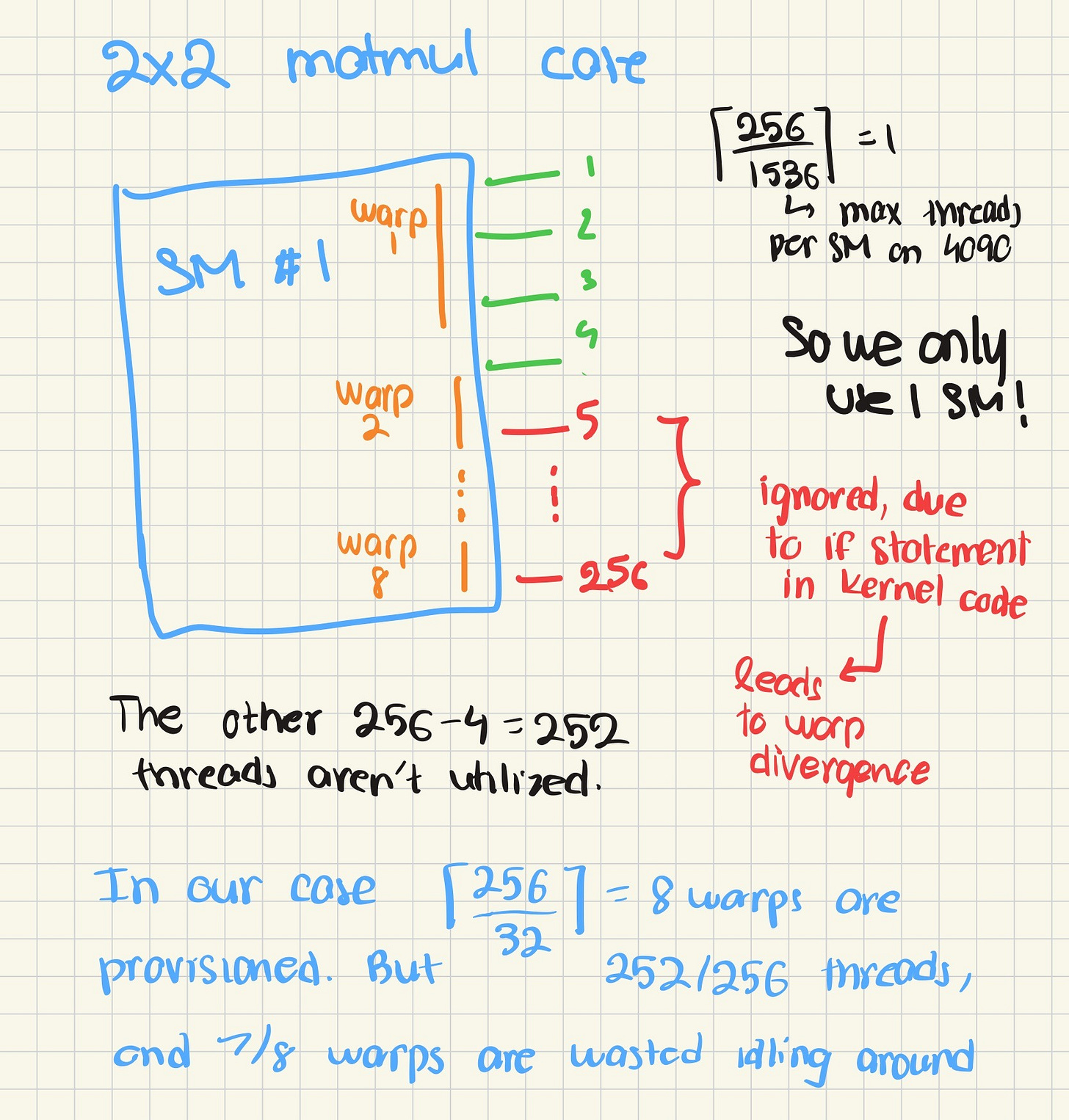
This GPU’s warp size is 32. In general, that’s a magic number for NVIDIA GPU products. Most NVIDIA GPUs, including the H100 and B100 have this. And in general, the threadblock —> warp partitioning is really just serializing their threadIdx across the x, y, and z dimension.
Here’s a formula to think about the mapping:
flat_id = threadIdx.x + threadIdx.y * blockDim.x + threadIdx.z * blockDim.x * blockDim.y
warp_id = flat_id / 32
Warps give us a finer granularity to also think about inefficiencies. Remember that tiling inefficiency? We can quantify it more precisely. In reality, each 256 thread thread block we create leads to 256 threads / 32 threads per warps = 8 warps being run. And since 7 out of 8 warps are idling, we’ve burned over 80% of the compute we’ve scheduled.
That’s why it’s important to differentiate between compute and useful compute. A critical part of optimization is making sure that we maximize this “goodpute” as much as we can.
What does the memory layout of a GPU look like?
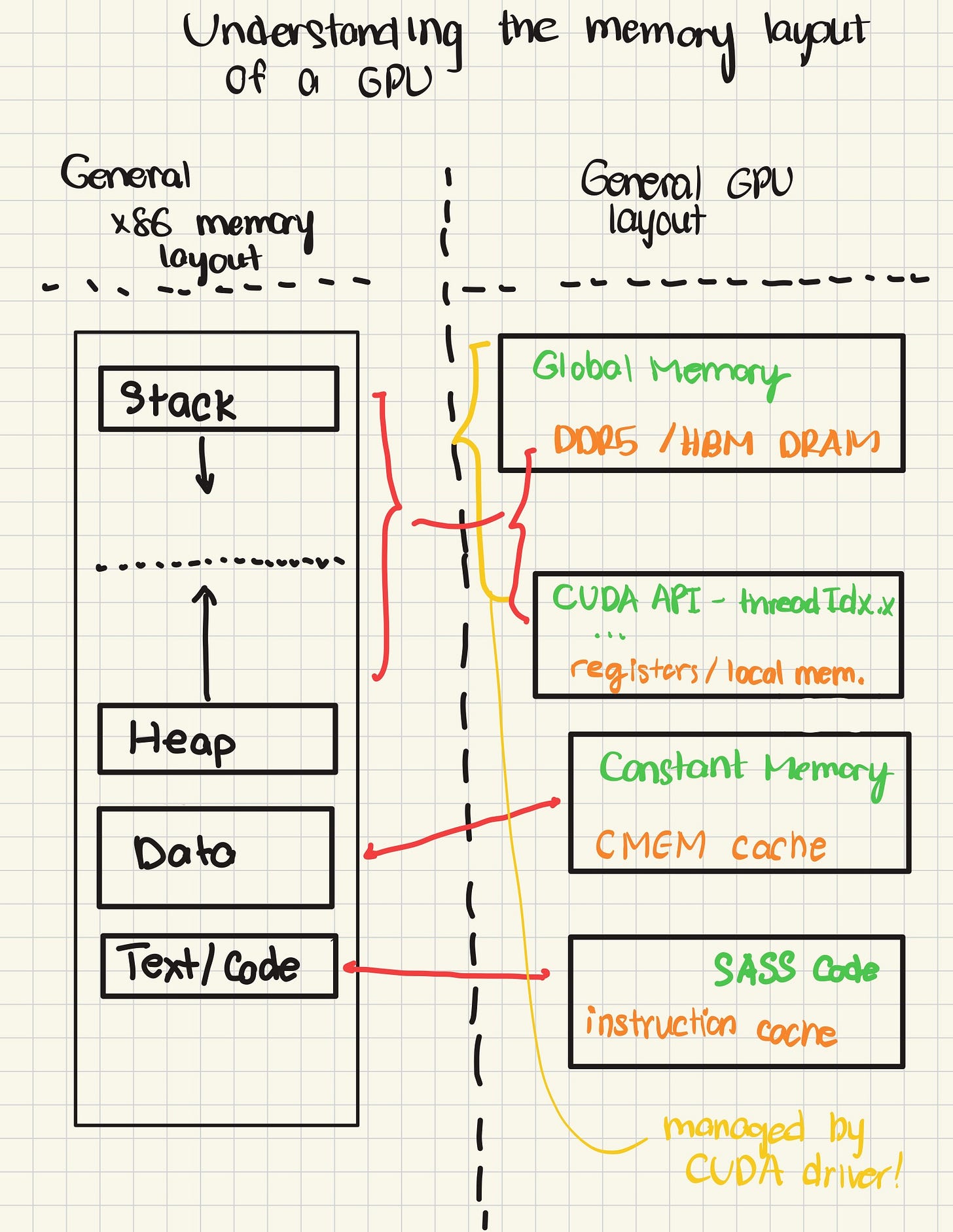
If you’ve taken a college course on computer architecture, you may have briefly glanced over GPUs. And after some point of taking operating systems or your first low-levels course, you may have thought about an tricky little question — why didn’t I ever hear about stacks, heaps, and data for GPUs? While I don’t have the complete answer to that, I’ll try to unearth some of the basic differences between CPU-backed virtual memory abstractions and the abstractions for a GPU.
Unlike the CPU, GPU memory abstractions are designed to be ad-hoc. The general process of setting up a kernel call is (1) allocate all the arrays into GPU memory, (2) issue parameters on the command queue, (3) wait for the GPU to complete running the kernel. In principle, this sounds a lot like how virtual memory works, with faint echos of calling convention: in virtual memory, (1) you can leverage malloc to place memory on the heap, (2) issue parameters to some registers from which the callee method may retrieve the arguments, and (3) once a method is done, control is returned to the caller.
But that’s also where cracks begin to emerge. Unlike CPUs, you cannot allocate large global pointers inside of a GPU kernel. In fact, all global memory has to be previously allocated. Additionally, nesting kernels isn’t too popular and is minimally supported, reducing the need to make CUDA abstractions sophisticated enough to justify support. The argument for why one shouldn’t nest kernels appears to be performance related - having to schedule a kernel while running a kernel is very inefficient in hardware.
That being said, we may be able to draw some parallels between the two abstractions to better understand how a GPU runs it’s kernels. Just like we maintain a text/code section to store instructions that we execute, the GPU stores instructions in an instruction cache, backed by global memory. Similarly, to quickly retrieve information about the kernel (parameters, thread / block configuration) that’s running, the GPU maintains a constant cache (CMEM) that can be thought of like the globals / static / data section. The constant cache stores things such as pointers to the various kernel arguments in device global memory, and constant parameters like matrix dimensions, CUDA API constants, and thread / block / grid configuration.
Finally, the global memory, alongside registers, can be thought of as a simplified version of dynamic memory controlled by the heap. All memory allocations must be provided through an API analogous to malloc on CUDA, making them effectively dynamic.
Overall, the puzzle pieces for building the virtual memory abstraction conceptually exist, but haven’t really been aligned together in a manner that’s completely comparable to the CPU. But attempts at making sophisticated memory abstractions off these puzzle pieces are definitely around.
What is this “DMA” buzzword you’ve been throwing around?
Great question, glad you’re curious. Direct Memory Access (DMA) engines are pieces of hardware dedicated to streamlining large memory transfers. Typically, without a DMA engine, peripheral devices like the GPU would need to force the CPU to perform the memory transfer.
Why’s that bad? Because this is how a CPU does a memory transfer, say from disk to RAM, at a high level. Let’s say we want to transfer a megabyte.
Load byte 1
Write byte 1
Load byte 2
Write byte 2
...
Load byte 1,000,000
Write byte 1,000,000
See how that can be slow? Essentially, the CPU is bound by having very precise read/write granularity. Because the CPU only reads, say, a byte (generally, it’s more) serially, we’ve burned a lot of time forcing the CPU to chip away at large volumes of data.
Here’s what a DMA copy engine (which allows for memory copies from things such as from L1 Cache to L2 Cache, aka LLC) enables for.
SET UP AN INTERRUPT
COPY BYTES FROM 0xDEADBEEF to ADDRESS 0xCAFEBEEF of size 1 MB
ISSUE DMA REQUEST

... do other useful work ...

... still using time ...

(Interrupt appears)

Return and process moved data on RAM
Especially since modern CPUs leverage techniques such as out-of-order processing (we do instructions out of order, literally when we can) and superscalar instruction fetching (fetching more than one instructions, with branch prediction) with multithreading (having register files for each thread), this allows the CPU to issue a transfer, context-switch over to perform work on other threads while setting up a mechanism to finish up it’s work after then interrupt, and then execute said mechanism once the DMA transfer is complete.
The idea is similar to GPUs. Rather than having each CUDA or Tensor core execute it’s own load and have to do a manual, byte by byte load, the GPU has a set of copy engines that enable the GPU to fire a request, temporarily forget and do some other task, and then return once DMA has indicated the request has been fulfilled.
Alright, fine. Let’s get to the point. DMA memory transfers matter because they serve as an option the hardware uses to accelerate I/O, and escape the memory bound.
Let’s talk bottlenecks. Generally speaking, the easiest way to speed up your computer is to cut out the slowest part, i.e the bottleneck. In this type of analysis, our goal is to constantly identify which component that our software workload uses creates a bottleneck.
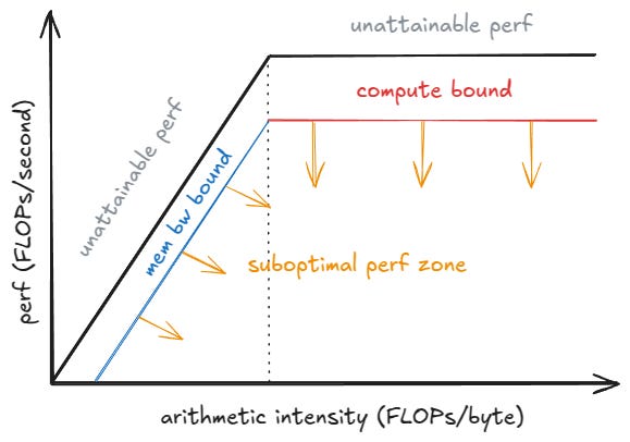
In general, workloads are either bound by (1) how fast their network, RAM/disk/memory/cache, etc. can fetch data or (2) how long it takes them to crunch through computation in their given precision (say, fp16 for inference or bf16 for pretraining). The former is termed the memory bound, and the latter the compute bound. If you’re interested in this sort of analysis, check out roofline analysis!
Benchmarking GPU memory transfer bandwidths, or having an expectation of how fast IO transfers are via DMA are good to think about how reads and writes to large matrices (I’m looking at you, attention!) can impact your overall performance. In the case of pre-training, for example, that performance metric can be loosely defined as the iteration time of a forward and backward pass. In inference, that may be prefill-based time to first token (TTFT), or decode based time per output (TPOT). To understand how to measure these, check out Aleksa Gordic’s blog on vLLM!
Roofline Analysis of GEMMs using our 4060 GPU
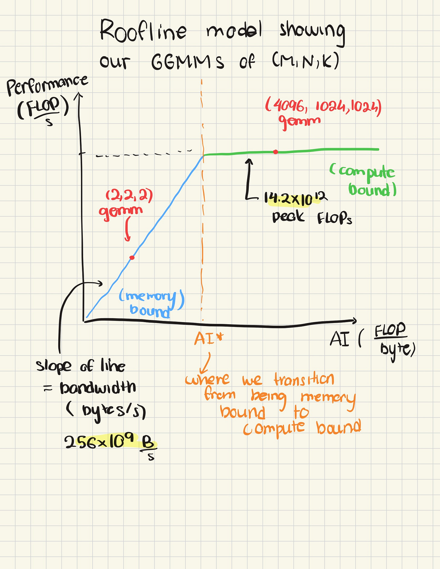
We wish to figure out whether running our General Matrix Multiplication (termed GEMM in industry) workload is either theoretically bound by memory, or compute. Let’s do that!
According to a technical website, my 4060 GPU achieves at most 14.6 TFLOPs, while bandwidth is 256 GB / s.
Running a benchmark for a matrix A of dimensions (1024 x 4096) multiplied by a (4096 x 1024) matrix B takes on average (across 10 trials) on FP32, 64 ms.
Let’s compute our arithmetic intensity first. How do we define FLOPs for a GEMM? In general, for each element, we count one FLOP for the add, and one flop for the multiplication. There are 2 FLOPS * M * N * K entries.
Applying this formula, we obtain -
2 * 1024 * 4096 * 1024 = 8589934592
How many bytes do we load? We load A and B once, do the matmul, and then write back to C. Assuming this, the bytes written formula is something as follows:
[M * K (A matrix) + K * N (B matrix) + M * N (C matrix)] * 4 bytes (for FP32)
Plugging:
4096 * 1024 + 4096 * 1024 + 1024 * 1024 = 9437184 * 4 =
Leading to an arithmetic intensity of 8589934592 / 37748736 ~ 227
Cool! We found an arithmetic intensity. But we need more context to understand what this number means.
Let’s figure out at which theoretical arithmetic intensity do we transition from memory bound to compute bound. Bandwidth (abbr. BW) has units (B / s) and Arithmetic Intensity (abbr. AI) has units (FLOP / B). So, BW * AI has dimensions of FLOP / s, or FLOPs.
Using this relationship, we’ll see at what arithmetic intensity does the memory bound equal the compute bound.
BW * AI* = peak compute FLOPs
AI* = peak compute FLOPs / BW
Plugging in numbers for the 4060, we obtain AI* = 14.6 * 1012 / 256 * 109 ~ 57
Since 227 » 57, we can safely assume that this GEMM workload on my hardware should be compute bound.
What about our 2x2 GEMM example above?
FLOP = 2 * 2 * 2 * 2 = 16
Bytes = (2 * 2 + 2 * 2 + 2 * 2) * 4 = 48
AI = 16/48 < 1
As this is under our AI* of 57, roofline analysis suggests we should expect to be memory bound for this workload.
What’s all this talk about DDR, GDDR, and HBM?
I’ve thrown the terminology of DDR4/5, GDDR6, and HBM (3E) around. Let’s take a surface level stab at what’s going on here, and what to expect in terms of differences with the three standards.
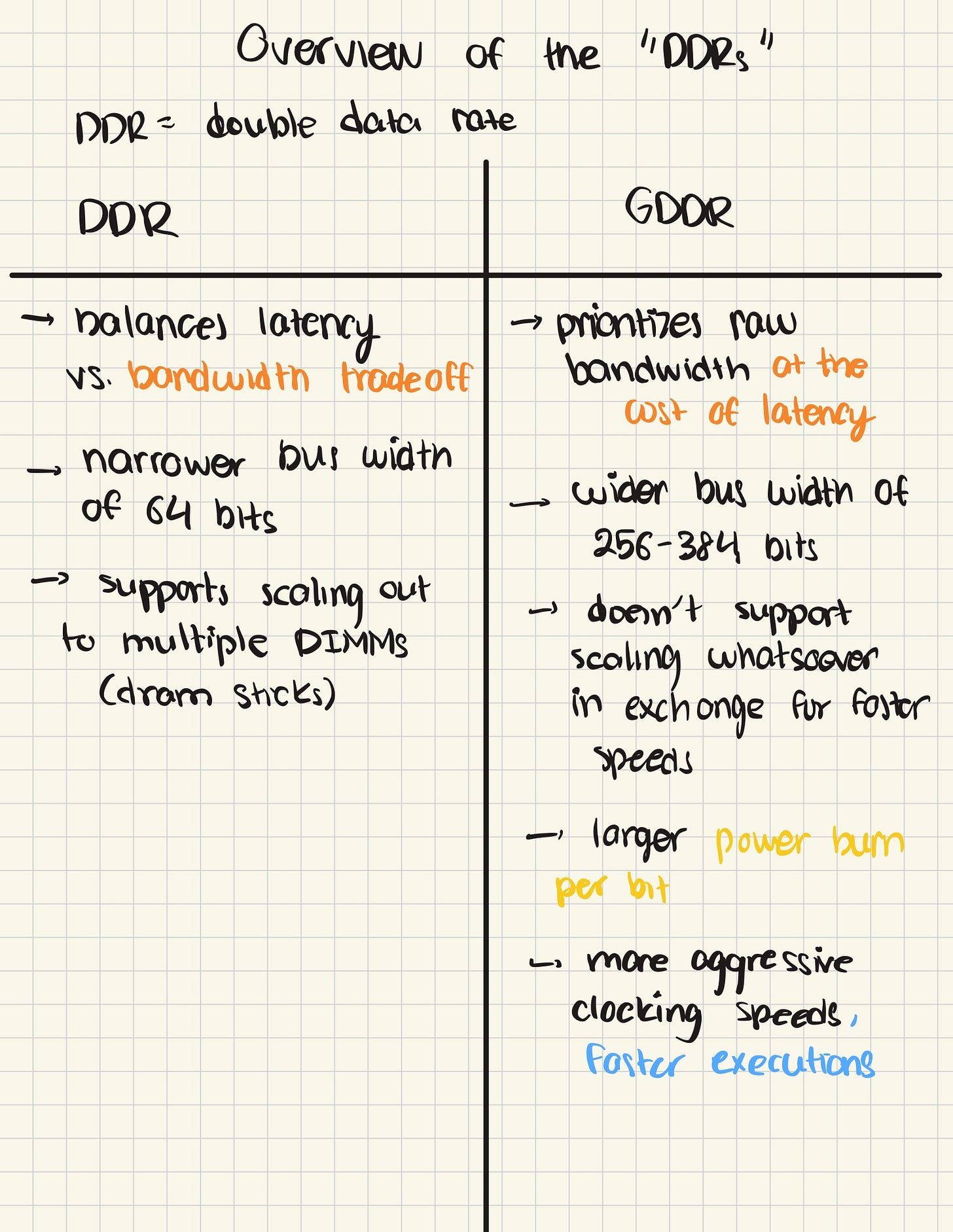
First, let’s differentiate between DDR, and GDDR. Double Data Rate memory is a standard that enables us to “double pump” memory. Generally, we assume in hardware that events happen either at the rising edge or falling edge of a clock cycle. DDR pushes this idea to the extreme — in exchange for more aggressive timing constraints, we enable a data transfer to happen at the rising AND falling edge of a clock cycle, effectively doubling the number of transfers we can do.
One thing I’d like to point in the hopes of making numbers make more sense real quick is how do we compute bandwidth from transfers. Roughly, you can assume that at each transfer, we share at most the number of bits as dictated by the bus width.
So, your effective bandwidth is equivalent to:
(transfers / second) * (bits / transfer) [this is your bus width] * (1 byte / 8 bits) [to arrive at standard units)
Hopefully this makes it easier to gauge memory performance. Now, back to DDR vs GDDR. DDR is primarily designed for hardware like cores and CPUs. GDDR, or Graphics Double Data Rate extends this concept to GPUs.
GPUs are much more power hungry than their CPU counterparts, as a result of having many, many more hardware wires in parallel for the comparable CPU counterpart. To optimize for this, GDDR trades off extensibility for better performance, fixing the number of Dual In-Line Memory Module DIMMs (aka one unit of DRAM). Unlike DDR, GDDR only lets you support only the number of DIMM sticks that you start out with. In exchange, you have significantly higher bus widths and faster clock speeds, which lead to better performance.
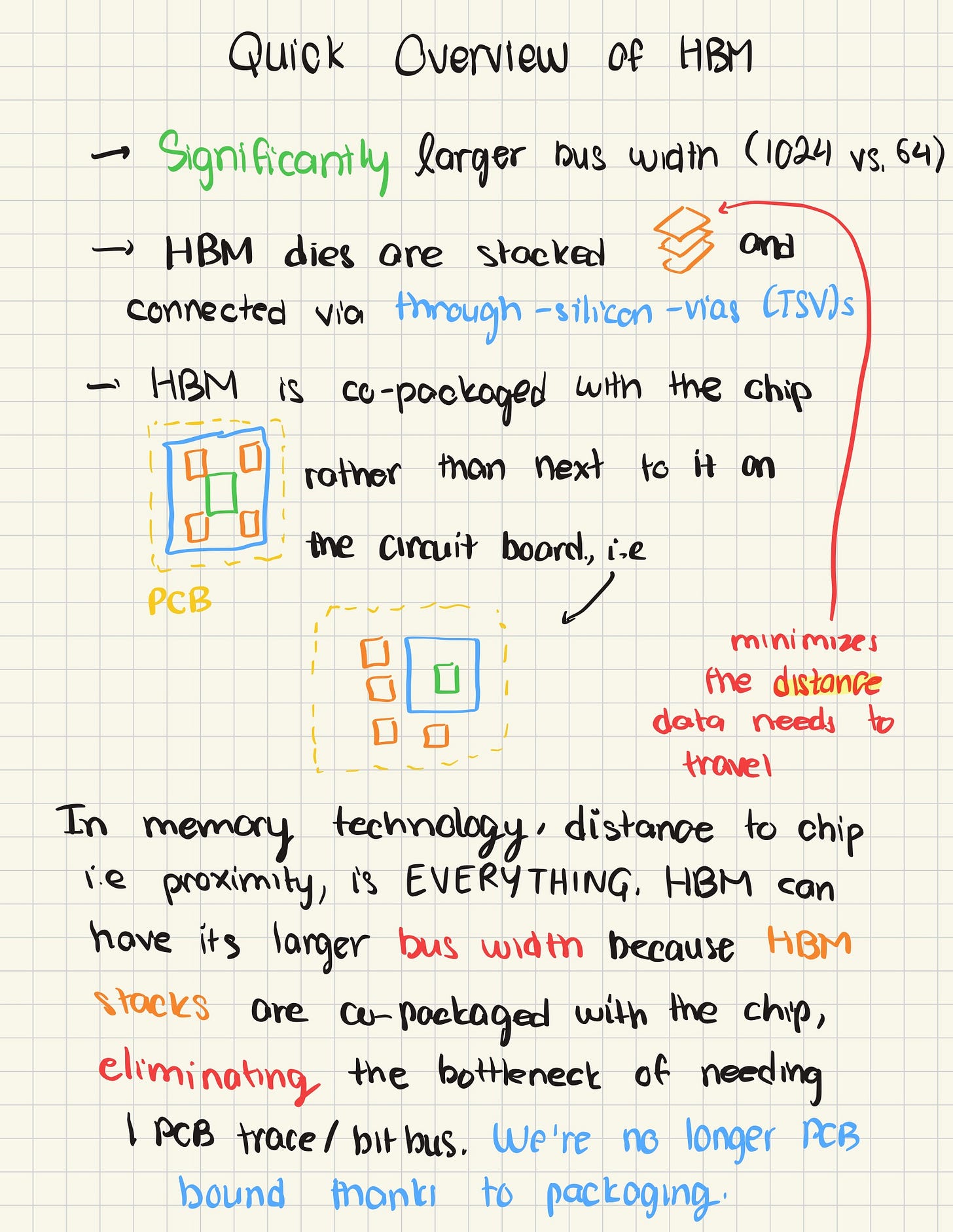
Can we do better? The answer turns out to be yes! GDDR and DDR both have to be externally connected to the chip on a PCB, fundamentally limiting their bus width. Enter HBM, which uses novel packing techniques to cut out this limitation.
Unlike DDR and GDDR-like standards, we now package the memory with the chip itself! This was revolutionary at its time, as breaking past PCB constraints using through silicon vias (TSVs) meant higher bandwidth, and in general, faster execution speeds in comparison to DDR components just because of how much fundamentally closer to the chip you are. However, this memory is also significantly more expensive than the two DDR standards, and as a result, it’s hard to find it in GPUs designed for anything but performance critical workloads.
Here’s a brief overview of the bandwidths for each memory protocol. We’ll use the latest standards (as of November 2025) for each as a basis for comparison.
HBM3E: 1 TB / per HBM stack
GDDR7: 900 GB / s (384 bit bus)
DDR5: 150-200 GB/s, assuming 4 channels
Acknowledgements
This was my first technical ~ish blog, and there’s a lot of people who took time out of there day to help me spot inconsistencies through this mammoth of a piece. And I’d like to take a moment to thank everyone who contributed to this for their time, and their valuable, amazing input.
I’d like to thank Michal Malyska for providing valuable feedback on the visual diagrams, helping me identify critical flaws that impeded readability, and pointing out useful pieces of information to include within sections in the Appendix. Similarly, I’d like to thank Lucy Revina for insightful feedback, and probing questions on the initial analogies, as well as challenging assumptions I had when coming up with discussion on AI cluster failures.
References
https://www.aleksagordic.com/blog/matmul
https://developer.nvidia.com/blog/using-shared-memory-cuda-cc/
http://docs.nvidia.com/cuda/cuda-c-programming-guide/index.html#simt-architecture
https://docs.nvidia.com/cuda/cuda-c-programming-guide/index.html#virtual-memory-management
https://www.aleksagordic.com/blog/vllm


